2011-5-25 17:2:32
views
The aluminum foil that makes up the plates in the electrolytic capacitor is treated in a few different processes to make it work properly and more efficiently. The most important process is the anodizing of the foil. Anodizing is a process that forms a very thin layer of aluminum oxide on one or both sides of the foil when the foil is immersed in an acidic solution and direct current is applied to the foil (one lead of the DC power supply is connected to the foil and the other is connected to a conductive plate in the acidic solution). This layer of aluminum oxide is the dielectric (insulator) and serves to block the flow of direct current. To increase the surface area on the foil (and ultimately increase capacitance), the foil can be etched by a chemical process. This would be done before the anodizing.
2011-5-23 17:10:18
views
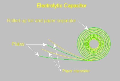
Electrolytic caps are more complex than film capacitors and are generally used for larger capacitance values (0.47 microfarad and higher). The electrolytic capacitor generally consists of 2 layers of aluminum foil with a layer of paper material between the plates. It looks a little like this:
2011-5-20 11:18:4
views
When a DC voltage source is applied to a capacitor there is an initial surge of current, when the voltage across the terminals of the capacitor is equal to the applied voltage, the current flow stops. When the current stops flowing from the power supply to the capacitor, the capacitor is 'charged'. If the DC source is removed from the capacitor, the capacitor will retain a voltage across its terminals (it will remain charged). The capacitor can be discharged by touching the capacitor's external leads together. When using very large capacitors (1/2 farad or more) in your car, the capacitor partially discharges into the amplifier's power supply when the voltage from the alternator or battery starts to fall. Keep in mind that the discharge is only for a fraction of a second. The capacitor can not act like a battery. It only serves to fill in what would otherwise be very small dips in the supply voltage.
2011-5-18 10:56:28
views
Vibration Test:
Test condition E for 720P, test condition B all others; no mechanical damage, short, open or intermittent circuit.
Moisture Resistance:
The hermetically sealed units shall be tested as outlined in the Moisture Resistance testing of section J. As a result of the test there shall be:
- No visible damage
- Max. ∆ C of ± 0.25%
- Min. IR = 33% of initial limit
- Max. DF = 0.12%
2011-5-16 16:40:5
views
Capacitive reactance (symbol Xc) is a measure of a capacitor's opposition to AC (alternating current). Like resistance it is measured in ohms, Ω, but reactance is more complex than resistance because its value depends on the frequency (f) of the electrical signal passing through the capacitor as well as on the capacitance, C.
| Capacitive reactance, c = | 1 | where: | Xc = reactance in ohms (Ω)
f = frequency in hertz (Hz)
C = capacitance in farads (F) |
| 2πfC |
The reactance Xc is large at low frequencies and small at high frequencies. For steady DC which is zero frequency, Xc is infinite (total opposition), hence the rule that capacitors pass AC but block DC.
For example a 1µF capacitor has a reactance of 3.2kΩ for a 50Hz signal, but when the frequency is higher at 10kHz its reactance is only 16Ω.
Note: the symbol Xc is used to distinguish capacitive reactance from inductive reactance XL which is a property of inductors. The distinction is important because XL increases with frequency (the opposite of Xc) and if both XL and Xc are present in a circuit the combined reactance (X) is the difference between them.
2011-5-13 17:49:11
views
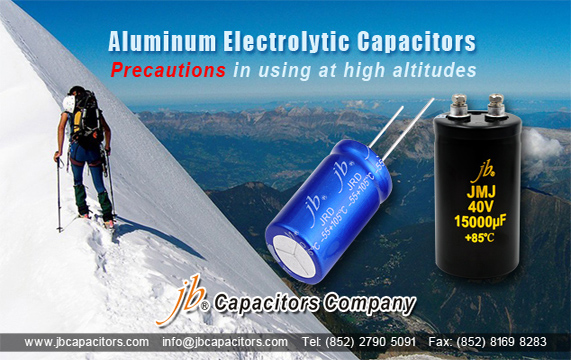
Here are precautions in using aluminum electrolytic capacitors at high altitudes, such as in
mountainous regions and in aircrafts.
As the altitude rises, the air pressure decreases. Therefore, if the capacitor is used at high altitudes, the atmospheric pressure becomes lower than the internal pressure of the capacitor. Due to the
construction of the aluminum electrolytic capacitor, there is no concern in using them at altitudes lower than about 10,000 (m).
2011-5-11 22:51:53
views
A run capacitor is a particular type of capacitor. A run capacitor uses the charge stored in the dielectric in order to boost the electrical current providing power to an electric motor. This type of capacitor is created to maintain a charge during constant use of the motor. These capacitors are often found in devices, such as heaters, that are continuously running.
One variety of run capacitor is often used in air conditioners. This type of run capacitor is called a dual run capacitor, and uses two run capacitors for two different functions. In an air conditioner, for example, one run capacitor is used to boost the fan motor, and another is used to boost the compressor motor.
Run capacitors typically are classified at 370 or 440 volts. It is necessary to ensure that the correct rating of run capacitor is installed in an engine. If a run capacitor with an incorrect voltage rating is installed in a motor that requires a capacitor for second-phase energy, it will throw off the magnetic field. An uneven magnetic field will cause the rotor to slow in the uneven spots, which increases energy noise, as well as power consumption, and can also cause performance problems and overheating issues.
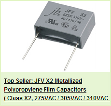
2011-5-9 22:47:1
views
This capacitor is small, with long lifespan and good self-healing ability. It is widely used as the start-up and running capacitor, especially for micro water pumps, cleaning machines, washing machines, and single-phase water pump motors.
Features:
jb film capacitors offers a full voltage range, from 63VDC to 2000VDC; our high voltage film capacitors include JFP (epoxy coating dipped type) and JFQ (box type) two series. JFA mylar polyester film capacitors, 1000V, 1200V is very popular. Also AC voltage and DC voltage both available, AC type film capacitors include JFC (AC metallized polyester film capacitors), JFN & JFO X2 class and JFT X1 class......
Tolerance range: ±1%, ±2%, ±2.5%, ±5%, ±10%
Temperature range: normally film capacitors temperature range is -40'C to 85'C, for some series we can provide a wide temperature range up to 125'C.
jb film capacitors technology available: winding technology and stacked technology (JFJ mini box series); single side metallized structure and double sided metallized structure (JFQ series) Safety Approvals of film capacitors: UL, TUV, CE, VDE...., X2 class, X1 class
Packaging: Ammo packaging and Bulk packaging both available, and all jb film capacitors are RoHS compliant
2011-5-6 13:37:20
views
For reflow, use thermal conduction systems such as infrared radiation (IR) or hot blast. Vapor heat
transfer systems (VPS) are not recommended.
Observe proper soldering conditions (temperature, time, etc.).
Do not exceed the specified limits.
Temperature measuring method: Measure temperature in assuming quantitative production, by sticking the thermo-couple to the capacitor upper part with epoxy adhesives.
Consult us for additional reflow restrictions.

2011-5-4 23:4:35
views
For reflow, use thermal conduction systems such as infrared radiation (IR) or hot blast. Vapor heat transfer systems (VPS) are not recommended.
Observe proper soldering conditions (temperature, time, etc.).
Do not exceed the specified limits.
Temperature measuring method: Measure temperature in assuming quantitative production, by sticking the thermo-couple to the capacitor upper part with epoxy adhesives.
Consult us for additional reflow restrictions.