2011-1-29 21:27:56
views
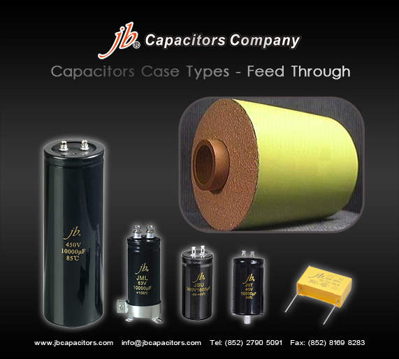
Round Feed Through capacitors, in a skin tight plastic wrap with solderable ends (Style Q). The hole in the center of the capacitor is either a Teflon Tube, Paper Tube or Phenolic Tube ranging in sizes from just a wire to a large threaded stud to fit through. The majority of Feed Throughs are custom made to exact customer requirements. They are very popular in filter applications.
2011-1-28 21:22:28
views
jb Capacitors are encased in a molded epoxy/plastic shell with epoxy fill. Available in Axial Leaded, Rectangular (Style E); Radial Leaded, Rectangular (Style F); and Axial Leaded, Round (Style T).

2011-1-27 21:18:59
views
Capacitors are wrapped in a skin tight plastic tape and then filled with epoxy on the ends. The most economical of the packaging methods. Available in Axial Leaded, Oval (Style W); Axial Leaded, Round (Style R); Radial Leaded, Oval (Style V); and Radial Leaded, Round (Style U). Special terminal configurations and sizes are also available.
2011-1-26 16:38:23
views
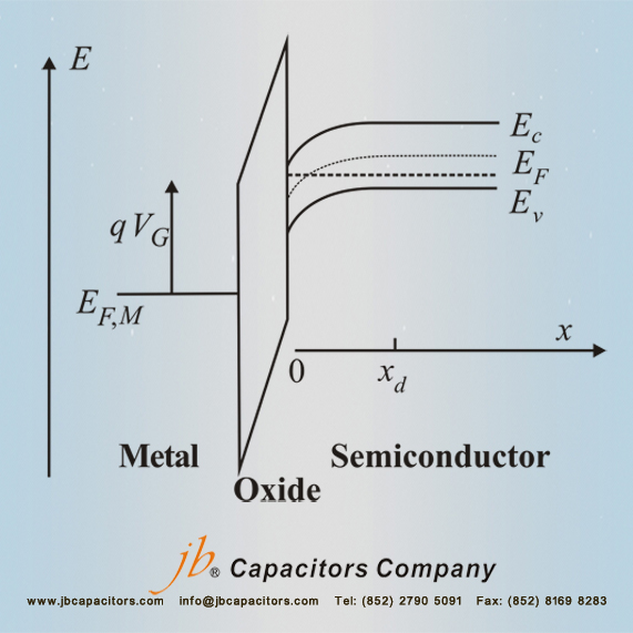
The flatband diagram is by far the easiest energy band diagram. The term flatband refers to fact that the energy band diagram of the semiconductor is flat, which implies that no charge exists in the semiconductor. The flatband diagram of an aluminum-silicon dioxide-silicon MOS structure is shown in Figure 6.2.4. Note that a voltage, VFB, must be applied to obtain this flat band diagram. Indicated on the figure is also the work function of the aluminum gate, FM, the electron affinity of the oxide, coxide, and that of silicon, c, as well as the bandgap energy of silicon, Eg. The bandgap energy of the oxide is quoted in the literature to be between 8 and 9 electron volt. The reader should also realize that the oxide is an amorphous material and the use of semiconductor parameters for such material can justifiably be questioned.
The flatband voltage is obtained when the applied gate voltage equals the workfunction difference between the gate metal and the semiconductor. If there is a fixed charge in the oxide and/or at the oxide-silicon interface, the expression for the flatband voltage must be modified accordingly.
Learn more about jb capacitors company:http://www.jbcapacitors.com/
.jpg)
Figure: Flatband energy diagram of a metal-oxide-semiconductor (MOS) structure consisting of an aluminum metal, silicon dioxide and silicon.
2011-1-25 16:27:51
views
The energy band diagram of an n-MOS capacitor biased in inversion is shown in below Figure. The oxide is modeled as a semiconductor with a very large bandgap and blocks any flow of carriers between the semiconductor and the gate metal. The band bending in the semiconductor is consistent with the presence of a depletion layer. At the semiconductor-oxide interface, the Fermi energy is close to the conduction band edge as expected when a high density of electrons is present. The semiconductor remains in thermal equilibrium even when a voltage is applied to the gate. The presence of an electric field does not automatically lead to a non-equilibrium condition, as was also the case for a p-n diode with zero bias.
For more products information please check: http://www.jbcapacitors.com/
2011-1-24 13:22:22
views
The MOS capacitor consists of a Metal-Oxide-Semiconductor structure as illustrated by Figure 1. Shown is the semiconductor substrate with a thin oxide layer and a top metal contact, referred to as the gate. A second metal layer forms an Ohmic contact to the back of the semiconductor and is called the bulk contact. The structure shown has a p-type substrate. This will refer to as an n-type MOS or nMOS capacitor since the inversion layer - as discussed in section 2 - contains electrons.

To understand the different bias modes of an MOS capacitor we now consider three different bias voltages. One below the flatband voltage, VFB, a second between the flatband voltage and the threshold voltage, VT, and finally one larger than the threshold voltage. These bias regimes are called the accumulation, depletion and inversion mode of operation. These three modes as well as the charge distributions associated with each of them are shown in Figure 2.
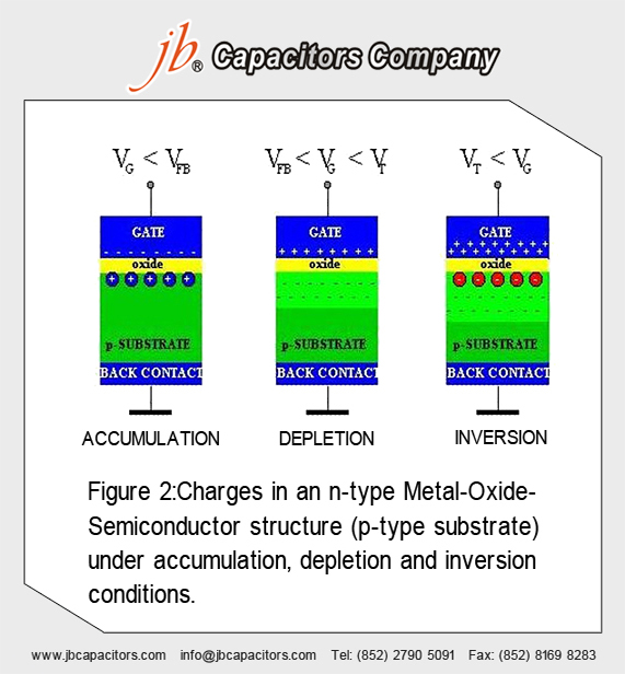
Accumulation occurs typically for negative voltages where the negative charge on the gate attracts holes from the substrate to the oxide-semiconductor interface. Depletion occurs for positive voltages. The positive charge on the gate pushes the mobile holes into the substrate. Therefore, the semiconductor is depleted of mobile carriers at the interface and a negative charge, due to the ionized acceptor ions, is left in the space charge region. The voltage separating the accumulation and depletion regime is referred to as the flatband voltage, VFB. Inversion occurs at voltages beyond the threshold voltage. In inversion, there exists a negatively charged inversion layer at the oxide-semiconductor interface in addition to the depletion-layer. This inversion layer is due to the minority carriers that are attracted to the interface by the positive gate voltage.
2011-1-24 13:18:52
views
'SMD' means Surface Mount Device. SMDs are components with small pads instead of leads for their contacts. They are designed for soldering by machine onto specially designed PCBs and are not suitable for educational or hobby circuits constructed on breadboard or stripboard.
2011-1-21 2:4:52
views
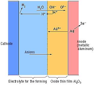
[2]-3 Electrolyte
Aluminum electrolytic capacitors are made by layering the electrolytic paper between the anode and cathode foils, and then coiling the result. The process of preparing an electrode facing the etched anode foil surface is extremely difficult. Therefore, the opposing electrode is created by filling the structure with an electrolyte. Due to this process, the electrolyte essentially functions as the cathode. The basic functional requirements for the electrolyte are as follows:
- (1) Chemically stable when it comes in contact with materials used in the anode, cathode, and electrolytic paper.
- (2) Easily wets the surfaces of the electrode.
- (3) Electrically conductive.
- (4) Has the chemical ability to protect the anode oxide thin film and compensate for any weaknesses therein.
- (5) Low volatility even at high temperatures.
- (6) Long-term stability and characteristics that take into consideration such things as toxicity.
2011-1-20 1:52:14
views
[2]-2 Forming (Anode Oxidation)
The "Forming" process is defined by creating an electrically insulating oxide (to provide the withstand voltage) on the aluminum surface by performing anode oxidation in the electrolytic solution used for the growth. The produced chemical film is used as the anode thin film.
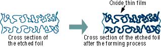
The anode oxidation, as follow shown, is produced by applying a voltage to the submerged foil found in the electrolytic solution used for growing the oxide film. Generally, the electrolytic solution is an aqueous solution such as ammonium boric acid, ammonium phosphate, or ammonium adipic for acid.
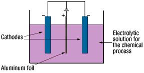
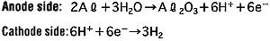
During the anode oxidation (DC electrolysis), AL2O3 is produced by a reaction between the water and the aluminum's Al3+ ions. The thickness of the grown thin film is nearly proportional to the applied voltage] with approximately 1.0 to 1.4 nm per volt. The chemical reactions on the anode side and the cathode side are as follows.
Below photographs show a magnified view of the oxide layer produced through anode oxidation.
| Low-voltage forming foil | High-voltage forming foil |
| 
| 
|
| Photograph of surface | Photograph of surface |
2011-1-19 18:58:59
views
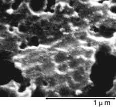
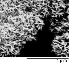
[2]-1 Surface Roughing (Etching)
The raw foil for the anode uses a high-purity aluminum foil (a minimum purity level of 99.99%) that is normally 50 to 100 m thick. The cathode foil material uses an aluminum foil that is at least 99% pure and about 15 to 60 m thick. Because the capacitance is proportional to the surface area of the electrodes, the effective surface area is increased by roughening (etching) the surface of the aluminum foil before growing the dielectric film. Generally, this surface roughening is referred to as "etching."
There are two typical etching processes. The first option submerges the aluminum foil in hydrochloric acid (physical etching). A secondary option is electrolysis where the aluminum as the anode is placed in an aqueous hydrochloric acid solution (electrochemical etching). In electrochemical etching, the etching profile will vary depending on factors such as the waveform of the electrical current, the composition of the solution, and the temperature. The etching method can be determined by the desired capacitor performance. Generally, it is possible to achieve etching multipliers (the ratio between the surface area of the smooth foil and the effective surface area of the etched foil) approximately between 3 and 120.
The foil is then rinsed thoroughly with water. Any residual chlorine ions on the foil's surface after etching can corrode the foil and damage the capacitor. After etching, the foil's surface can be categorized broadly as shown below by the selected voltage at which the capacitor functions properly. See the magnified view of the surface in below photograph.
| | Foil Surface
(3500x Magnification) | Cross-section of Capacitor
(350x Magnification) |
Types of
Etched Foils | Low-voltage foil |  |  |
| High-voltage foil |  |  |