jb Introduce MOS Capacitors Structure and Principle of Operation
The MOS capacitor consists of a Metal-Oxide-Semiconductor structure as illustrated by Figure 1. Shown is the semiconductor substrate with a thin oxide layer and a top metal contact, referred to as the gate. A second metal layer forms an Ohmic contact to the back of the semiconductor and is called the bulk contact. The structure shown has a p-type substrate. This will refer to as an n-type MOS or nMOS capacitor since the inversion layer - as discussed in section 2 - contains electrons.

To understand the different bias modes of an MOS capacitor we now consider three different bias voltages. One below the flatband voltage, VFB, a second between the flatband voltage and the threshold voltage, VT, and finally one larger than the threshold voltage. These bias regimes are called the accumulation, depletion and inversion mode of operation. These three modes as well as the charge distributions associated with each of them are shown in Figure 2.
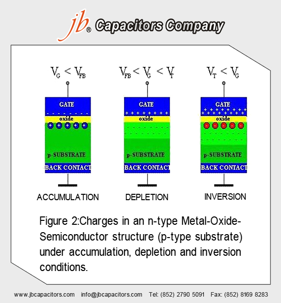
Accumulation occurs typically for negative voltages where the negative charge on the gate attracts holes from the substrate to the oxide-semiconductor interface. Depletion occurs for positive voltages. The positive charge on the gate pushes the mobile holes into the substrate. Therefore, the semiconductor is depleted of mobile carriers at the interface and a negative charge, due to the ionized acceptor ions, is left in the space charge region. The voltage separating the accumulation and depletion regime is referred to as the flatband voltage, VFB. Inversion occurs at voltages beyond the threshold voltage. In inversion, there exists a negatively charged inversion layer at the oxide-semiconductor interface in addition to the depletion-layer. This inversion layer is due to the minority carriers that are attracted to the interface by the positive gate voltage.


0 Comment so far
Leave a reply