jb Energy Band Diagram of an MOS Structure Biased in Inversion
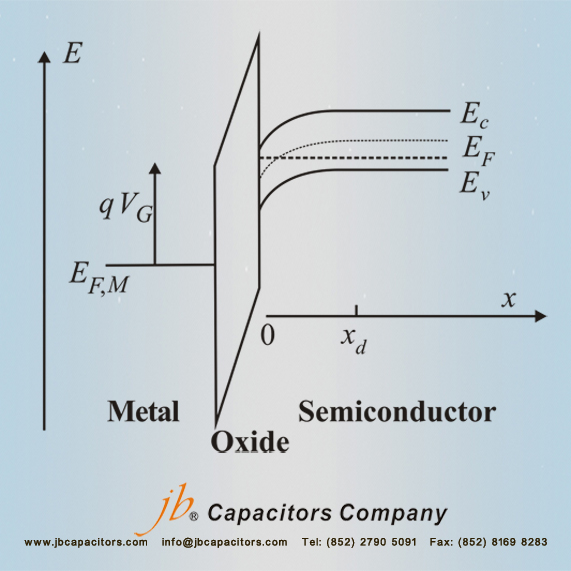
The energy band diagram of an n-MOS capacitor biased in inversion is shown in below Figure. The oxide is modeled as a semiconductor with a very large bandgap and blocks any flow of carriers between the semiconductor and the gate metal. The band bending in the semiconductor is consistent with the presence of a depletion layer. At the semiconductor-oxide interface, the Fermi energy is close to the conduction band edge as expected when a high density of electrons is present. The semiconductor remains in thermal equilibrium even when a voltage is applied to the gate. The presence of an electric field does not automatically lead to a non-equilibrium condition, as was also the case for a p-n diode with zero bias.
For more products information please check: http://www.jbcapacitors.com/