2011-1-24 13:22:22
views
The MOS capacitor consists of a Metal-Oxide-Semiconductor structure as illustrated by Figure 1. Shown is the semiconductor substrate with a thin oxide layer and a top metal contact, referred to as the gate. A second metal layer forms an Ohmic contact to the back of the semiconductor and is called the bulk contact. The structure shown has a p-type substrate. This will refer to as an n-type MOS or nMOS capacitor since the inversion layer - as discussed in section 2 - contains electrons.

To understand the different bias modes of an MOS capacitor we now consider three different bias voltages. One below the flatband voltage, VFB, a second between the flatband voltage and the threshold voltage, VT, and finally one larger than the threshold voltage. These bias regimes are called the accumulation, depletion and inversion mode of operation. These three modes as well as the charge distributions associated with each of them are shown in Figure 2.
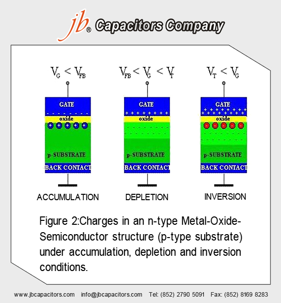
Accumulation occurs typically for negative voltages where the negative charge on the gate attracts holes from the substrate to the oxide-semiconductor interface. Depletion occurs for positive voltages. The positive charge on the gate pushes the mobile holes into the substrate. Therefore, the semiconductor is depleted of mobile carriers at the interface and a negative charge, due to the ionized acceptor ions, is left in the space charge region. The voltage separating the accumulation and depletion regime is referred to as the flatband voltage, VFB. Inversion occurs at voltages beyond the threshold voltage. In inversion, there exists a negatively charged inversion layer at the oxide-semiconductor interface in addition to the depletion-layer. This inversion layer is due to the minority carriers that are attracted to the interface by the positive gate voltage.
2011-1-24 13:18:52
views
'SMD' means Surface Mount Device. SMDs are components with small pads instead of leads for their contacts. They are designed for soldering by machine onto specially designed PCBs and are not suitable for educational or hobby circuits constructed on breadboard or stripboard.
2011-1-13 22:55:25
views
Glass capacitors can find applications in many areas as a result of their performance characteristics. They do tend to be specialist components and are normally fairly costly.
Circuits exposed to temperature extremes: With the tolerance to a wide range of temperatures, both high and low, some circuits that may be exposed to very harsh environmental conditions may choose to use glass capacitors. Not only can they withstand high and low temperatures, but they do not change value at these extremes by a great amount. Accordingly remote sensors may choose to use glass capacitors.
Applications requiring a high Q circuit: Many circuits including oscillators and filters may require high Q components to give the required performance. Filters will be able to attain their required bandwidth, and for oscillators there are a number advantages including improvement of phase noise performance, reduction in drift and reduction of spurious oscillations.
Low microphony requirements: It may be expedient to use glass capacitors in circuits where microphony may be a problem. RF oscillators including those found in phase locked loops and PLL synthesizers may benefit from their use.
High power amplifiers: The high current capability of glass capacitors may enable their use in RF power amplifiers where other forms of capacitor would not be suitable.
High tolerance areas: In many areas such as filters or free running oscillators the high tolerance and precision accompanied by the low temperature coefficient may be required to maintain the tolerances within a precision circuit.
2011-1-12 22:51:29
views
The construction of glass dielectric capacitors is relatively straightforward to understand. The capacitor consists of three basic elements: the glass dielectric, aluminium electrodes and the encapsulation. However the assembly of the glass capacitors is undertaken in a manner that ensures the required performance is obtained.
As the capacitance between two plates is not always sufficient to provide the required level of performance, the majority of capacitors use a multiplayer construction to provide several layers of plates with interspersed dielectric to give the required capacitance.
Although the glass plates are always flat, and tubular forms of construction are not applicable, the glass capacitors are usually available with leads emanating in either a radial or axial form. Essentially the leads either exit the encapsulation at the side or the end.http://www.jbcapacitors.com/
2011-1-11 23:37:24
views
Glass capacitors offer several advantages over types of capacitor. In particular glass capacitors are applicable for very high performance RF applications:
Low temperature coefficient : Glass capacitors have a low temperature coefficient. Figures of just over 100 ppm / C are often obtained for these capacitors.
No hysteresis : Some forms of capacitor exhibit hysteresis in their temperature characteristic. This is not the case for glass capacitors which follow the same temperature / capacitance when the temperature is rising and falling.
Zero ageing rate : Many electronics components change their value with age as chemical reactions take place within the component. Glass capacitors do not exhibit this effect and retain their original value over long periods of time.
No piezo-electric noise : Some capacitors exhibit the piezo-electric effect to a small degree. This can result in effects such as microphony on oscillators. Where this could be a problem, the use of glass capacitors could help solve the problem.
Extremely low loss / High Q : Glass capacitors are very low loss as there is virtually no dielectric loss. This enables very high Q circuits to be built using them. provided the other components (e.g. inductors) are not lossy.
Large RF current capability : Some capacitors are not able to withstand large values of current. This is not the case for glass capacitors which are suitable for use in RF high power amplifiers, etc.
High operating temperature capability : Glass dielectric capacitors are able to operate at very high temperatures. Many are able to operate at temperatures up to about 200C without fear of damage or performance shortfall.
2011-1-10 23:34:4
views
Glass capacitors are used where the ultimate performance is required for RF circuits. Glass dielectric capacitors offer very high levels of performance, although their cost is high when compared to many other forms of capacitor. Typically a glass capacitor will have a relatively low capacitance value. The values of glass capacitors may range between a fraction of a picofarad up to two to here thousand picofarads. As such these capacitors are used mainly in radio frequency circuit design.
While the performance of glass capacitors is exceedingly high, this is also usually reflected in the cost - it can run into many pounds or dollars for each component. As such glass dielectric capacitors are reserved only for the most exacting RF requirements, often on low volume products where cost is not such an issues as it is in high volume products. The supply of glass capacitors is also limited to a small number of manufacturers and suppliers, and the capacitors may not be available ex-stock.
2011-1-8 1:43:56
views
Mass produced electronic circuit boards need to be manufactured in a highly mechanized manner. The traditional leaded electronic components do not lend themselves to this approach. Although some mechanisation was possible, component leads need to be pre-formed, and when they were inserted into boards automatically problems were often encountered as wires did not fit properly slowing production rates considerably.
It was reasoned that the wires that had traditionally been used for connections were not actually needed for printed circuit board construction. Rather than having leads placed through holes, the components could be soldered onto pads on the board instead. This also saved the need to drilling as many holes in boards.
As the components were mounted on the surface of the board, rather than having connections that went through holes in the board, the new technology was called surface mount technology or SMT. The idea for SMT was adopted very quickly because it enabled greater levels of mechanisation to be used, and it considerably saved on manufacturing costs.
2011-1-6 22:43:45
views
In theory, capacitors can be coupled both in series and parallel. If you need a 100MF cap and have two at 50MF, you can connect them in parallel, and that will give you 100MF (and same voltage rating as each). If you couple them in series, you get half the capacitance, and double voltage rating. But coupling electrolytic capacitors in series to get higher voltage rating must generally be discouraged. For this to work, you must be sure that the two (or more) caps share the voltage load properly; a resistor network can augment this, but if leakage currents are markedly different or the capacitors age differently, you are looking at a potential disaster, so do this only as a last resort, if at all.
2010-12-25 13:32:55
views
Integrated circuits: There is a variety of packages which are used for integrated circuits. The package used depends upon the level of interconnectivity required. Many chips like the simple logic chips may only require 14 or 16 pins, whereas other like the VLSI processors and associated chips can require up to 200 or more. In view of the wide variation of requirements there is a number of different packages available.
For the smaller chips, packages such as the SOIC (Small Outline Integrated Circuit) may be used. These are effectively the SMT version of the familiar DIL (Dual In Line) packages used for the familiar 74 series logic chips. Additionally there are smaller versions including TSOP (Thin Small Outline Package) and SSOP (Shrink Small Outline Package).
The VLSI chips require a different approach. Typically a package known as a quad flat pack is used. This has a square footprint and has pins emanating on all four sides. Pins again are bent out of the package in what is termed a gull-wing formation so that they meet the board. The spacing of the pins is dependent upon the number of pins required. For some chips it may be as close as 20 thousandths of an inch. Great care is required when packaging these chips and handling them as the pins are very easily bent.
Other packages are also available. One known as a BGA (Ball Grid Array) is used in many applications. Instead of having the connections on the side of the package, they are underneath. The connection pads have balls of solder that melt during the soldering process, thereby making a good connection with the board and mechanically attaching it. As the whole of the underside of the package can be used, the pitch of the connections is wider and it is found to be much more reliable.
A smaller version of the BGA, known as the microBGA is also being used. As the name suggests it is a smaller version of the BGA.


 -butyrolactone