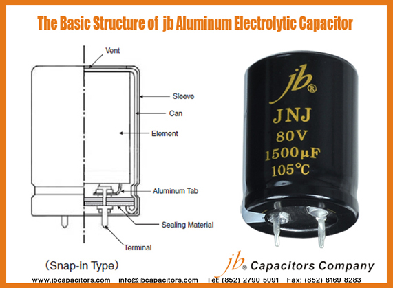
jb Structure of Aluminium Electrolytic Capacitors

Basic construction:
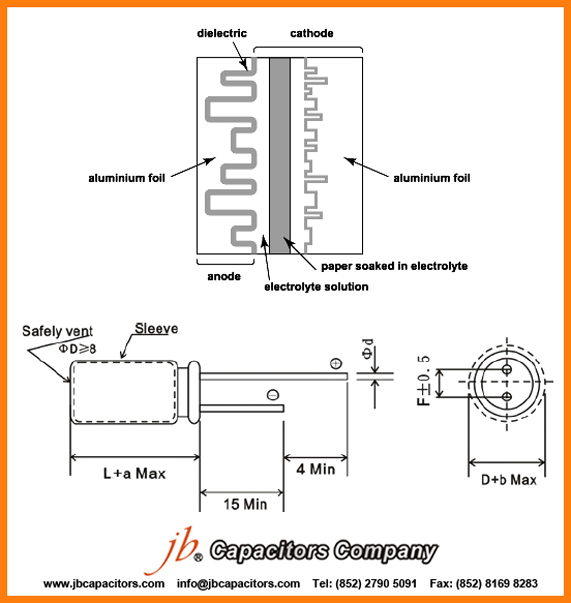
1, Two pieces of foils interleaved with an absorbent paper build up the key element of an Aluminium Electrolytic Capacitor, and all these materials should be wound tightly into a cylinder shape
2, The positive foil, or the anode foil are all made from pure aluminium foil. The aluminium oxide dielectric has been formed electrolytically on the surface.. 
3, The foil has been etched to make the effective surface area more larger, and the area of the anode is usually 30–100 times larger than the plan area of the foil.

Figure: How dielectric structure works in an Aluminium Electrolytic Capacitor ?
4, The other plate is a combination of high-absorption paper impregnated with an electrolyte, in contact with a cathode foil. 
5, The electrolyte is there to make good contact with the anode, by permeating its etched structure, and also to repair any flaws in the oxide layer when the capacitor is polarised. 
6, The function of the aluminium cathode foil is to reduce the series resistance of the capacitor by making contact with the paper over a wide area.

We welcome you to order our jb Aluminium Electrolytic Capacitors and anatomy it, if you want to have a more clear understanding of them. Do it yourself will be more fun and meaningful.

jb Tell You The Basic Structure of An Aluminum Electrolytic Capacitor

jb Capacitors manufactures and markets Aluminum Electrolytic Capacitors, including Snap-in Type 
Aluminum Electrolytic Capacitors, Screw Type Aluminum Electrolytic Capacitors, Lug Type Aluminum 
Electrolytic Capacitors and Leaded Radial Aluminum Electrolytic Capacitors , also SMD Aluminum Electrolytic Capacitors.

Today we would like to share with the the basic structure of  jb Snap-in Type Aluminum Electrolytic Capacitors. 

1, The most important part is the Core , or called as element. 
Aluminum electrolytic capacitor winding core is made of aluminum foil anode, electrolytic paper, aluminum foil cathode , electrolytic paper, totally made four layers overlap;

2, The Can or Case, witch is made of aluminum material.

3, The Sleeve. usually insulating sleeve is made by PVC or PET material and with different colors. The most common color is black.

4, The Terminal. For snap in type, the terminal usually are two pins. But still with different lead out portion types, like wire, chips, screws. 

5, The Sealing Materail . Rubber stopper (EPDM rubber, butyl rubber), lug cover (needle cover, U-shaped lug cover), screw the cover (cover phenolic resin, polyphenylene sulfide resin Cover)

jb Introduce MOS Capacitors Structure and Principle of Operation

The MOS capacitor consists of a Metal-Oxide-Semiconductor structure as illustrated by Figure 1. Shown is the semiconductor substrate with a thin oxide layer and a top metal contact, referred to as the gate. A second metal layer forms an Ohmic contact to the back of the semiconductor and is called the bulk contact. The structure shown has a p-type substrate. This will refer to as an n-type MOS or nMOS capacitor since the inversion layer - as discussed in section 2 - contains electrons.

To understand the different bias modes of an MOS capacitor we now consider three different bias voltages. One below the flatband voltage, VFB, a second between the flatband voltage and the threshold voltage, VT, and finally one larger than the threshold voltage. These bias regimes are called the accumulation, depletion and inversion mode of operation. These three modes as well as the charge distributions associated with each of them are shown in Figure 2.

Accumulation occurs typically for negative voltages where the negative charge on the gate attracts holes from the substrate to the oxide-semiconductor interface. Depletion occurs for positive voltages. The positive charge on the gate pushes the mobile holes into the substrate. Therefore, the semiconductor is depleted of mobile carriers at the interface and a negative charge, due to the ionized acceptor ions, is left in the space charge region. The voltage separating the accumulation and depletion regime is referred to as the flatband voltage, VFB. Inversion occurs at voltages beyond the threshold voltage. In inversion, there exists a negatively charged inversion layer at the oxide-semiconductor interface in addition to the depletion-layer. This inversion layer is due to the minority carriers that are attracted to the interface by the positive gate voltage.